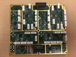
rf circuit board be repaired
RF circuit boards require unique printed circuit board materials that fulfill specific requirements for high frequency operation. The material must have a high dielectric constant, low signal losses and be consistent over a wide range of temperatures. It also must have a good coefficient of thermal expansion and good mechanical properties. In addition, the conductive copper layer must be able to carry heavy currents without being damaged by excessive heat.
Typical RF circuits are multi-layered with the copper traces being separated by dielectric materials. They are also designed with a group plane or power plane, which is used to conduct power and grounding between layers. This helps prevent electrical interference and allows the traces to be narrower and faster. In addition, the RF circuit board design must be able to meet performance requirements for different impedance matching methods. These include series and shunt impedance matching, which use capacitors or inductors in parallel with the line, L-section matching, which uses a combination of both, and T-section matching, which uses an inductor connected to a resistor in a T shape.
The first step to repairing an rf circuit board is to inspect the damaged area for signs of damage. Visual inspection can reveal broken traces, soldering errors, tombstoning, excessive solder on joints and cracks in the PCB. A comparison with a known good board can help determine the cause of the failure. The next step is to test the circuit for continuity and voltage, using appropriate tools on a static-free bench.
A common source of RF circuit board failure is trace damage, which can prevent electricity from flowing through the track. Trace damage can be caused by corrosion, oxidation or even mechanical stress. Fortunately, most trace damage can be repaired by simply melting the existing solder with a soldering iron and cleaning the area.
Can rf circuit board be repaired if damaged?
In cases of more serious or widespread trace damage, the conductive copper layer may need to be replaced on the affected area. Several common RF circuit board materials are available, including Rogers and FR-4 laminates. They differ in their characteristics, such as the coefficient of thermal expansion, dielectric constant and loss tangent. These factors should be considered by RF designers when choosing a conductive copper thickness and material for the PCB.
RF circuit board repair kits are available to make the process easier. They typically contain a variety of hand tools and desoldering braid. The kit should also include a power supply and an oscilloscope to help identify problems with the circuit board.
Before the soldering process, it’s important to clean the area with a cloth soaked in rubbing alcohol to remove any contaminants that could cause short circuits. Once the contaminant has been removed, the existing solder on the pad should be removed with a sharp knife or screwdriver. A tweezer can be used for small or odd-shaped pads.
Once the pad is cleaned, a new solder joint can be made by placing adhesive-backed copper tape over the repair site. Then the pads are positioned and soldered to the exposed copper. Once the solder has cooled, it can be inspected to verify proper alignment and positioning.